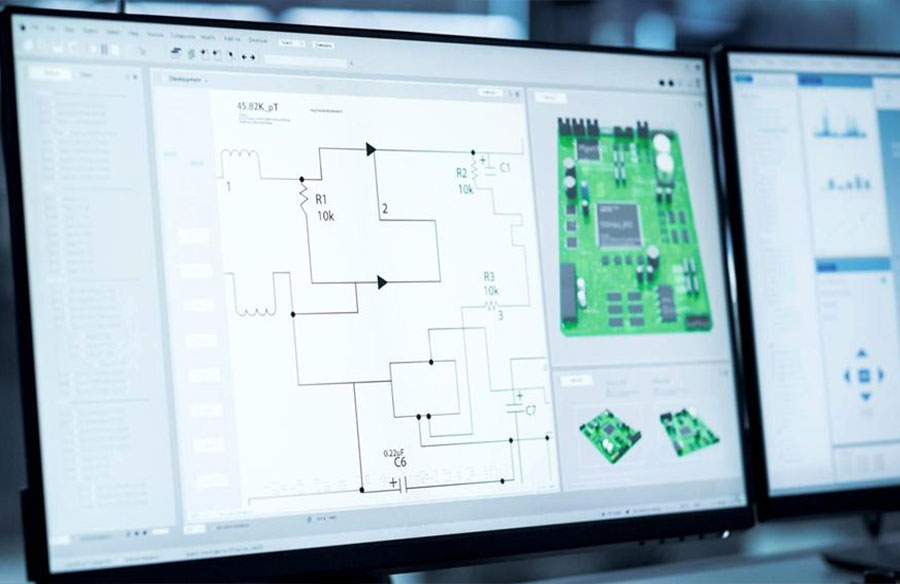
The manufacturing procedure of printed circuit boards (PCB) is usually complex to ensure the high quality and performance of the product. The printed circuit boards can either be of single or multiple layers. The process of fabrication differs in the number of layers. This is the reason why the structures of PCB differ and have different numbers of steps when it comes to its process of manufacturing. It can be said that design own PCB correlates with the complexity of the board. Reducing the number of steps may result in malfunctioning of the board or hurt its performance. However, when a PCB is designed perfectly and all steps are followed in its fabrication performs all tasks efficiently. This article is the ultimate step-by-step guide on how to design your own PCB board.
To design own PCB is necessary before initiating the fabrication process. Numerous computer-based software programs are available for your to design your own PCB board. The layout of the printed circuit board is building the actual circuit board.
1. Development of Parts in Computer Aided Design Software Library
Beginning with the development of CAD library files has different parts such as the layout of PCB footprints, schematic symbols, display schematics, and simulation models. After completion of the library files, build a logical circuit diagram. Computer-aided software is responsible for connecting the schematic sheet symbols. The simulation of the circuit ensures the electrical components’ design. After all these steps, tools for schematics give information about the connectivity of the board.
Designing the Layout
Nets are responsible for the connection of component pins. The designers are utilizing a sketch of the PCB for the arrangement of the footprint of the components. After these portions are optimized, planes and traces of pins of components are drawn. Computer-aided software governs spaces and widths. The traces of a net are not supposed to cross the traces of another net. Auto-routing is accomplished after the generation of output files and drawings to be manufactured. Building and designing your own PCB comprises the design of schematics and its simulation along with the creation of the DRC setup, placement of components, routing, making the power planes, bill of materials for assembly, and fabrication of the printed circuit board.
Creation of Schematics
Before starting the computer-aided software design of the printed circuit board, it is compulsory to complete the library of the parts to be designed. The design of a product necessitates logical symbols for all components to be placed on the circuit board such as resistors, connectors, inductors, and capacitors. Therefore, the components are first arranged over the board in a software and then these components are placed in a special arrangement, linked through wires in the schematics labeling each terminal and component. Every data circuit and memory is having nets usually single or more than one for the connection of nodes. For clarity, the schematic component requires component repositioning where needed.
Simulating the Circuit
Testing is performed after all of the connections and components are laid down. SPICE or any other tool is utilized for the confirmation of perfect simulation of the circuit. Designers and engineers can test the circuits with such computer-aided tools before its implementation on hardware. Such tools are critical in the design of printed circuit boards as these save time and budget.
Setting the Computer Aided Tool
Every tool used for designing printed circuit boards has its distinct capabilities and features that are utilized by designers. Guidelines on how to design own PCB are avoiding the net overlap and delivering spacing for components. Designing grids is among the techniques which is utilized for routing the traces and arrangement of components.
Creating the Design Layout of Component
The layout of the circuit board follows the database of design along with connectivity data of the schematics. First of all, the arrangement of the footprint of the components is made on the computer-aided tool as per the outline. When the footprint of the design is made, all of the net connections start appearing. The designers who are experienced enough always consider connectivity, physical impediments, electrical noise, and hotspots for instance, mounting hardware, connectors, and cables are arranging the components for optimal performance.
Routing
After the creation of the components layout, everything must be in its perfect spot. Therefore, now it is time for hooking up nets. To achieve this, links in the rubber-band nets are supposed to be transformed into planes over a piece of paper. This has become possible because of the tools available in the computer-aided programs comprising automated routing facilities for cutting down the design time to a great extent. However, routing must be done with extreme caution to ensure the efficient placement of nets for appropriate signal lengths and to avoid any noisy paths.
Making Wiring Paths
The integrated circuit installed on the circuit board has a requirement of connection to ground and power plane. Therefore, solid planes are created for such components to have proper access to power and ground paths. However, the creation of ground and power paths on such planes is not that easy. Such paths must also return signals being sent along all traces. These pathways may also generate certain noise and affect the performance of the designed circuit board if having numerous splits, cut-outs, and holes.
The Last Check
The design of the printed circuit board is considered complete after the placement of components is complete along with marking proper routing traces and planes for ground and power. Afterward, designing different markers and text is required that are to be silk screened over the outer layers along with the conduction of the final check for design rules. After you design your own PCB certain factors must be checked like copyright information, date, and names of different terminals and components. Manufacturing drawings must also be produced to be utilized during the fabrication and assembly.
2. Rules to Design your Own PCB
Numerous electronic devices require higher integration of semiconductor devices even though many contemporary and powerful circuit boards along with system-on-chips are being utilized in several applications. Still, the necessity of custom-printed circuit boards is not yet outdated. As far as one-time development is considered, a simple printed circuit board may also result in playing a critical role, and in the creation of novel electronic systems, PCBs always perform the core role. The following are some rules that must be followed to design PCB board.
Choosing Appropriate Grid Set
The designers can avoid interval settings even though multi-grid appears to be very functional. Designers are supposed to select the products that suit the application for which PCB is designed like for copper PCB polygon is critical. Therefore, the selection of an appropriate grid set can result in enduring circuit board performance and efficiency.
Direct Routing
Talking of direct routing may seem illogical but it has to be considered if you want to design your own PCB because short wiring and traces will result in better performance and reduce the complexity of the printed circuit board.
Utilization of Layer for Power
A lot of PCB designers favor designing the power layer to be of copper as it is easier and quicker to work on. However, current within the PCB can be easily dispersed throughout the circuit board and voltage can be supplied through ground return pathways ensured by connecting many wires in parallel.
Printed Circuit Board Imposition
For cutting down the expense and increasing the mass production of a prototype or working device, choosing the right size that works perfectly with the machinery of the manufacturer is of great value. Before duplicating the design, it must be taken to the circuit board layout over the panel and get the recommended size from the manufacturer.
Component’s Values Integration
The designer is suggested to opt for discrete components with both lower and higher values. One way of managing the bill of materials and decreasing expenses is through integration through a small standard value range.
Checking the Design Rules
The DRC or design rule check within the designing software of PCBs usually takes a couple of seconds for its execution but has a large impact on time saving. This is because regular review of the work will result in minimizing the chances of errors or even no errors and issues when you design your own PCB.
Checking Manufacturer Parameters of Printed Circuit Boards
To avoid confusion, Gerber files should be produced and used for verification of the design. Almost every computer-aided tool offers to download Gerber files for verification of the design.
Conclusion
When you design your own PCB, many factors can make it dysfunctional because of numerous technical and non-technical flaws. For example, wrong vias, wrong ground planes, wrong power planes, leakage resistances, voltage drops, and the influence of stray capacitance, etc. Therefore, there is a need to follow a standard procedure for designing the printed circuit board to ensure its perfect working when it is fabricated. This article highlights the important steps that are needed to be taken for the design of a printed circuit board along with consideration of certain rules that must be followed.
Viasion is a dynamic tech solutions provider at the forefront of innovation, specializing in PCB Assembly, design and manufacturing.